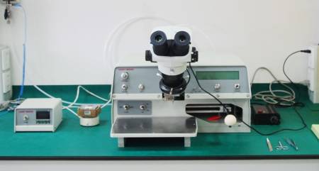
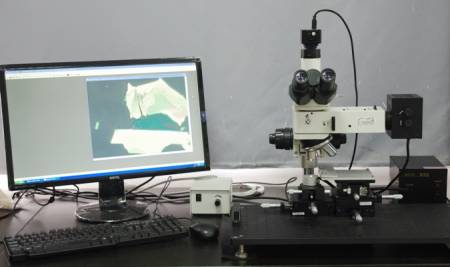
Cryogen-free variable temperature scanning tunneling microscope in ultrahigh vacuum
(home-made, Chinese Patent of Invention: ZL201410091094.8; RSI 87,063701(2016))
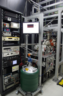


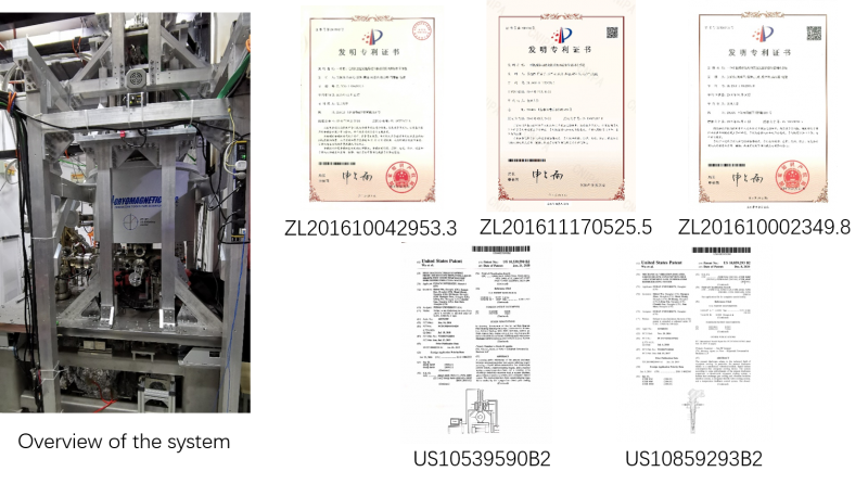
- left: overview of the system
- middle: closeup of the STM
- right: National invention patent certificate
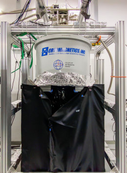
Cryogen-free low temperature ultrafast spin-polarized scanning tunneling microscope housed
in a room-temperature-bore vector superconducting magnet (home-made & patented)
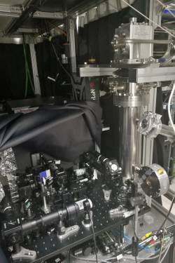
Ultrafast nano-optics characterization system

- left: tunable femtosecond laser system (spectra physics)
- middle: variable temperature laser scanning optical microscope (home-made)
- right: ambient sample-scanning confocal scanning optical microscope (custom-made)
Cryogen-free high magnetic field variable temperature optical microscope (home-made)


- left:7 T-2 T-2 T system
- middle:Out-of-plane 9 T system
- right:Out-of-plane 6 T system
Cryogen-free variable temperature optical cryostat (home-made)
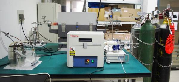
MBE system for growing low dimensional quantum materials (home-made)

Glovebox-E-Beam deposition-AFM system for sample preparation


wire bonder for wiring up electronic devices (West Bond)
optical microscope for dry transfer of 2D materials
various ovens for sample growth and treatment
plasma cleaner and UV ozone cleaner for sample preparation


shared equipments and facilities
- Nanofabrication facility at Fudan including e-beam lithography, photolithography, ebeam and thermal deposition, dry etchings, SEM, etc.
- State Key Laboratory of Surface Physics at Fudan including PPMS, XRD, AFM, etc.